Welcome to the Horn Law Motor Vehicle Accident Information Center
Original HTML

Welcome to the Horn Law Motor Vehicle Accident Information Center

Clear, practical information about motor vehicle injury claims, effective legal representation, and obtaining fair and full injury settlements and awards.

Clear Guidance for Every Stage After an Accident

What Do I Need to Understand?

What Should I Do Next?

How Can I Achieve the Best Possible Outcome?

Articles

When Does Uber’s Insurance Cover a Driver Waiting for a Ride in Missouri?

Your Uber Crash Claim Depends on Coverage During the App-On "Waiting" Period Key Takeaways: Missouri…

Douglas "Doug" Horn

October 21, 2026

What Counts as Flagrant Disregard in a Missouri Car Crash Claim?

When Reckless Driving Becomes Grounds for Punitive Damages in Missouri Key Takeaways: In a Missouri…

Douglas "Doug" Horn

October 17, 2026

Why Serious Teen Crash Settlements Over $35,000 Need Court Approval in Missouri

When a Teen’s Crash Settlement Needs a Judge’s Signature Key Takeaways: In Missouri, a settlement…

Douglas "Doug" Horn

October 13, 2026

How Much Is a Pinched Nerve Car Accident Settlement Worth in Missouri?

What Drives the Value of a Pinched Nerve Claim After a Missouri Crash Key Takeaways:…

Douglas "Doug" Horn

October 8, 2026

How to Prove an Uber Driver Was Heading to a Pickup Before a Missouri Crash

Proving Uber Period 2 Status After a Serious Missouri Crash Key Takeaways: Under Missouri’s TNC…

Douglas "Doug" Horn

October 4, 2026

How Missouri’s $1 Million Uber Policy Applies During an Active Ride

When the Meter Was Running: Understanding the Coverage That Applies to Your Uber Crash Key…

Douglas "Doug" Horn

October 3, 2026

What should I do after a car accident in Kansas City if I feel injured but didn’t go to the hospital right away?

Many people don’t recognize the full extent of their injuries until hours or even days…

Douglas "Doug" Horn

November 4, 2025

How do car accident attorneys handle insurance companies that try to reduce settlement offers?

Insurance companies often look for ways to minimize what they pay out, especially in cases…

Douglas "Doug" Horn

November 4, 2025

What types of injuries qualify for a personal injury claim after a vehicle accident?

A wide range of injuries may provide grounds to pursue a personal injury claim. These…

Douglas "Doug" Horn

November 4, 2025

Can I still pursue compensation if I was partly at fault for the accident in Kansas City?

In Missouri, accident victims may still seek compensation even if they were partially responsible for…

Douglas "Doug" Horn

November 4, 2025

What makes work injury claims different from other personal injury cases?

Work-related injuries, such as those from construction accidents, warehouse incidents, or industrial hazards, often fall…

Douglas "Doug" Horn

November 4, 2025

What should I do after a car accident in Kansas City if I feel injured but didn’t go to the hospital right away?

Many people don’t recognize the full extent of their injuries until hours or even days…

Douglas "Doug" Horn

November 4, 2025

How do car accident attorneys handle insurance companies that try to reduce settlement offers?

Insurance companies often look for ways to minimize what they pay out, especially in cases…

Douglas "Doug" Horn

November 4, 2025

What types of injuries qualify for a personal injury claim after a vehicle accident?

A wide range of injuries may provide grounds to pursue a personal injury claim. These…

Douglas "Doug" Horn

November 4, 2025

Can I still pursue compensation if I was partly at fault for the accident in Kansas City?

In Missouri, accident victims may still seek compensation even if they were partially responsible for…

Douglas "Doug" Horn

November 4, 2025

What makes work injury claims different from other personal injury cases?

Work-related injuries, such as those from construction accidents, warehouse incidents, or industrial hazards, often fall…

Douglas "Doug" Horn

November 4, 2025

What should I do after a car accident in Kansas City if I feel injured but didn’t go to the hospital right away?

Many people don’t recognize the full extent of their injuries until hours or even days…

Douglas "Doug" Horn

November 4, 2025

How do car accident attorneys handle insurance companies that try to reduce settlement offers?

Insurance companies often look for ways to minimize what they pay out, especially in cases…

Douglas "Doug" Horn

November 4, 2025

What types of injuries qualify for a personal injury claim after a vehicle accident?

A wide range of injuries may provide grounds to pursue a personal injury claim. These…

Douglas "Doug" Horn

November 4, 2025

Can I still pursue compensation if I was partly at fault for the accident in Kansas City?

In Missouri, accident victims may still seek compensation even if they were partially responsible for…

Douglas "Doug" Horn

November 4, 2025

What makes work injury claims different from other personal injury cases?

Work-related injuries, such as those from construction accidents, warehouse incidents, or industrial hazards, often fall…

Douglas "Doug" Horn

November 4, 2025

Motor Vehicle Accident? Make a FIRST CALL to Horn Law Firm, PC at (816) 795-7500 for Immediate Help

Frequently Asked Questions

Find clear, practical answers organized around the journey of someone injured in a motor vehicle accident—from the first steps after a crash through medical treatment, insurance claims, settlement, and lawyer selection.

The comprehensive FAQ Center provides answers to broader questions and helps visitors find related guides, videos, and educational resources. Each major Information Center page also includes focused FAQs addressing questions specific to that subject.

What Should I Do Immediately After an Accident?

How Does the Insurance Claim Process Work?

What Should I Know About Medical Treatment and Recovery?

How Are Injury Settlements and Compensation Determined?

How Do I Choose the Right Motor Vehicle Accident Injury Lawyer?

What to Do After a Car Accident Involving an Injury

The actions taken immediately after a car accident and during the days that follow can affect both medical recovery and an injury claim.

This resource explains important steps such as seeking appropriate medical care, preserving photographs and other evidence, reporting the collision, dealing with insurance companies, documenting injuries, and understanding when legal assistance may be appropriate.

How to Select a Motor Vehicle Accident Lawyer

Choosing a lawyer can affect how quickly an investigation begins, whether important evidence is preserved, how insurance coverage is identified, how medical evidence is developed, and how thoroughly the case is prepared for settlement or litigation.

This guide helps injured people understand what effective motor vehicle accident representation should include and what to consider before hiring a lawyer.

This educational guide will help injured people understand:

When hiring a lawyer may be appropriate

What effective motor vehicle accident representation should include

Why rapid response and early investigation matter

How strong injury cases are developed

What can influence settlement value

Which questions to ask before hiring a lawyer

What to look for when comparing law firms

The purpose of this guide is not simply to tell visitors to hire a lawyer. It is to help them evaluate legal representation and understand what a motor vehicle accident lawyer should do to protect an injury claim.

Early Legal Representation After a Motor Vehicle Accident Injury

The first few days after a motor vehicle accident can have a lasting impact on an injury claim.

Early legal representation can help preserve important evidence, begin the accident investigation, identify available insurance coverage, establish insurance claims, and address communications with insurance companies while the injured person focuses on medical recovery.

This resource explains the role early legal work can play in protecting an injury claim and laying the foundation for building a strong case.

What is My Motor Vehicle Injury Claim Worth?

A motor vehicle accident injury claim cannot be valued accurately from the type of collision or injury alone.

The value of a claim depends on the facts that can be documented and proven. Important considerations may include how the collision occurred, the degree of fault assigned to each party, the nature and permanence of the injuries, the medical treatment required, time lost from work, reduced earning ability, and the effect the injuries have on daily life.

In Missouri, fault attributed to an injured person may proportionally reduce the amount recovered. Available insurance coverage can also affect the practical recovery because automobile policies provide specific types of coverage with defined dollar limits.

Determining case value therefore involves more than adding medical expenses. It requires a careful review of accident evidence, medical records, treatment recommendations, wage documentation, insurance policies, and the long-term effect of the injuries.

This guide explains the major factors used to evaluate motor vehicle accident injury claims, why apparently similar accidents can have very different outcomes, and what may strengthen or weaken a claim.

Motor Vehicle Accident Cases: Videos that Inform

Watch practical videos explaining important motor vehicle accident, injury, insurance, and legal topics in a clear and accessible format.

The Horn Law Video Library provides another way for injured people and their families to understand the claims process and make informed decisions.

Videos are connected whenever possible to related Accident & Injury Guides and frequently asked questions, making it easy to move between written and video information.

Class (B2B/B2C)
Ignore
Ingest Status
Need Review
Dedupe hash
7db1fe7331cbe9ce7da54cc27c1dc59d
Press Eligible
No
Press Eligible Reason
Irrelevant (need review): Law firm promotional content about injury claims and legal representation.
Source Name
The Horn Law Firm, P.C
Content Hash (SHA-256, erste 32 hex)
cbec962bfa74efe341b336d66b8d53b8
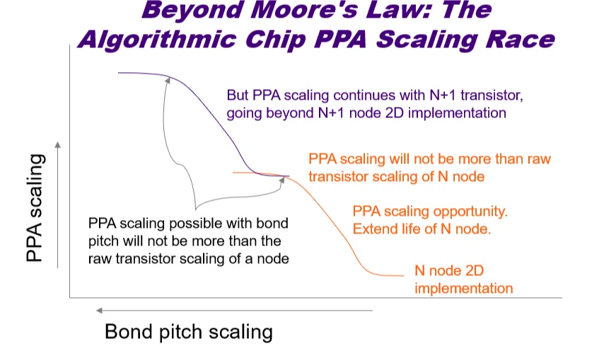
Beyond Moore’s Law: The Algorithmic Chip PPA Scaling Race That Was Already Underway
Image File
Original HTML

Beyond Moore’s Law: The Algorithmic Chip PPA Scaling Race That Was Already Underway

A recent semiconductor announcement has captured global attention — but the core ideas have deep roots in western academic research and design-methodology work across multiple firms, as reflected in public publications and patents.

Disclaimer: This article reflects the author’s personal professional perspective and is not intended to represent an official GlobalFoundries position. All technical references cited are publicly available. Any follow-up industry conversations will be coordinated consistent with GlobalFoundries policies.

The Announcement That Changed the Conversation

A semiconductor company’s “Tau Scaling Law” announcement in May 2026 introduced a new scaling framework — one that shifts attention from making transistors physically smaller to reducing signal delay across devices, circuits, chips, and systems. Coverage appeared in Reuters, CNBC, Nikkei Asia, Forbes, and The Register. Commentary has ranged from skeptical (“more branding than breakthrough”) to geopolitically significant (“a defining moment in the semiconductor bifurcation”).

Both reactions miss the deeper story.

The core thesis is straightforward: algorithmic and design-level scaling was not invented in 2026. What changed is the strategic importance of productizing it. The announcement is significant not because the concept is new, but because a design-driven scaling methodology is now being claimed as production-deployed across many chip variants.

In simple terms, Tau Scaling reframes chip scaling around time delay rather than geometry alone. Instead of relying primarily on smaller transistors, it seeks to reduce delay across devices, interconnects, circuits, chips, software, and systems through architecture, placement, routing, 3D integration, and hardware/software co-optimization.

The Western Footprint: Research That Was Always There

Consider two data points from the western technology ecosystem.

At the 2020 IEEE/ACM International Conference on Computer-Aided Design (ICCAD), researchers published a physical synthesis and post-layout optimization flow for monolithic design of 3D integrated circuits. The work demonstrated that stacking standard cells vertically — without shrinking the transistors themselves — could deliver up to 9 % smaller wirelength, 88 % improvement in timing slack, and 8.7 % lower power compared to conventional 2D designs. The core insight: better performance was achievable by changing how logic was spatially organized, not by demanding a new process generation from the foundry.

► "Pin-3D: A Physical Synthesis and Post-Layout Optimization Flow for Heterogeneous Monolithic 3D ICs," Proc. 39th ICCAD, ACM, Nov. 2020. DOI: 10.1145/3400302.3415720

A patent application filed with the United States Patent and Trademark Office in early 2024 covers a three-dimensional integrated circuit design methodology — specifically, how metal stack configuration and bonding pitch optimization interact to improve power, performance, and area (PPA). The approach describes two chips bonded face-to-face, with bonding pitch geometry directly driving PPA outcome.

► U.S. Patent Application No. 20250272465, “Three-Dimensional Integrated Circuit (3DIC) and 3DIC Design Method and System,” USPTO, filed February 2024. patents.google.com/patent/US20250272465A1

These are not isolated examples. They are representative of a sustained research and intellectual property trajectory in the western semiconductor ecosystem. The technical evidence comes from publications and patent filings; the broader strategic interpretation comes from industry analysis of how constraints change engineering priorities.

What Gets Built Under Pressure

A Forbes analysis published on Jun 27, 2026 frames this dynamic with precision. The author observes that “when best-in-class components are available externally, most firms source them externally. The cost of that efficiency is capability loss: they may never fully develop the internal muscle to align hardware, software, architecture and operations around one technical objective under pressure.”

► Mark Greeven, “What Huawei’s Chip Strategy Reveals About Innovation Under Pressure,” Forbes, June 27, 2026. forbes.com/sites/markgreeven/2026/06/27

This is the structural explanation for why the western ecosystem held the intellectual foundations — and did not build on them at scale. With access to extreme ultraviolet lithography and leading-edge foundry capacity, the path of least resistance was to let the transistor do the work. Algorithmic optimization was valuable as a complement to process scaling. It was not positioned, funded, or prioritized as a production-grade continuation of transistor scaling.

This is not a criticism, but a structural observation about how industries allocate attention and investment. When the dominant performance metric is transistor-based process-node progression, and when the supply chain reliably delivers new generations, the incentive to develop production-grade algorithmic alternatives is structurally limited.

The Forbes analysis adds a necessary nuance: constraint does not automatically create advantage — “more often, it creates delay, inefficiency, and technical debt” — and becomes strategically useful “only when an organization has enough engineering depth, resources, and market demand to convert constraint into discipline.” Productizing a complex design methodology across hundreds of chip variants over six years is exactly the kind of disciplined industrial execution that converts a research concept into a platform. Credit where it is due.

The Bifurcation Problem

The deeper concern is not whether any single company’s chip matches another’s on a specific benchmark. The deeper concern is what happens when export-constrained semiconductor ecosystems develop on divergent trajectories — different hardware, different software stacks, different EDA SW and methodologies, and importantly at different cost points.

The Forbes analysis identifies this directly: “Two AI compute ecosystems are now developing on separate trajectories, built on different hardware, different software stacks, different supply chains, and different assumptions.”

Recommended by LinkedIn

This bifurcation is visible in foundry market data. China’s share of advanced-node foundry revenue — which peaked near 30 % in 2019 — collapsed to approximately 12 % by 2025, driven by the cumulative effect of export control implementation. That collapse created precisely the industrial pressure that forced the algorithmic scaling path to production. The resulting ecosystem is now optimizing its software, models, and AI infrastructure around domestic hardware — not because it is superior by every metric, but because it is accessible.

As the Forbes analysis observes: “Adequacy within an accessible ecosystem can be worth more than optimality within one that is politically off-limits.”

For the global semiconductor industry, this is the inflection point. Algorithmic scaling approaches that improve PPA without requiring the next process node are no longer just a research direction. They are now being publicly claimed as production-scale methodologies — approaches that any ecosystem can study, adapt, and extend.

Why EDA and Algorithmic Solutions Were Structurally Underfunded

There is a structural reason why this class of solutions has not received investment commensurate with its technical potential.

Semiconductor technology leadership has historically been defined and communicated by materials science and device physics. Process roadmaps, conference keynotes, and investment theses are organized around the transistor as the atomic unit of progress. Electronic Design Automation (EDA) software and the algorithms that drive physical design have been positioned as infrastructure supporting the transistor’s trajectory — not as the lead driver of a parallel, and potentially complementary, scaling path.

The EDA industry has produced remarkable intellectual work for decades, while also carrying the burden of supporting the infrastructure required for leading transistor process-node scaling. When performance gains can be achieved by waiting for the next node, and when the supply chain reliably delivers new nodes, the business case for investing in production-grade algorithmic alternatives is structurally weaker. The research gets done in academic settings, but the investment to industrialize — to move from a compelling paper result to a commercial EDA flow — rarely follows at the same pace.

The result is a persistent gap between intellectual activity and commercial deployment. The 2020 ICCAD publication cited above, and the 2024 patent filing, both demonstrate that the western ecosystem was generating compelling work in this direction. What was missing was the industrial imperative to drive that work to production at scale.

What the Productization Moment Changes

The recent announcement changes the framing for the entire industry.

First, the EDA ecosystem has a clearer commercial signal. Supporting design-level scaling approaches is no longer a research bet. It is a demonstrated production requirement, with proven demand at volume across hundreds of chip variants.

Second, foundries that have invested in hybrid wafer bonding capability, fine-pitch interconnect technology, and 3D design-rule frameworks now have a more explicit value proposition for customers seeking performance beyond their current process node.

Third — and most urgently — the bifurcation problem makes this a strategic imperative. If the western ecosystem does not develop production-grade tools and methodologies for 3D monolithic design-driven scaling, it risks losing influence across key layers of the global semiconductor stack: silicon, IC design, software, and AI systems.

Class (B2B/B2C)
B2B
Ingest Status
Rewritten
Dedupe hash
06655f0ce525518d28a94e0ef2e58d41
Press Eligible
Yes
Press Eligible Reason
Manuelle Prüfung nötig. Risiko: MEDIUM. Flags: ['numbers']. Stichprobe: False
Source Name
GlobalFoundries Newsroom
Image URL
https://media.licdn.com/dms/image/v2/D5612AQHUEkjmtoYzXQ/article-cover_image-shrink_720_1280/B56Z8M54HWGcAQ-/0/1782627926719?e=2147483647&v=beta&t=FqJ63oayyH5epM61MvyjTgdwA8jQtogGQPX7fzEZ8p4
Content Hash (SHA-256, erste 32 hex)
33b13b42eb51760bcdae60ce88fb4f17
From Sand to Transistors: The Journey of Semiconductor Manufacturing
Image File
Original HTML

From Sand to Transistors: The Journey of Semiconductor Manufacturing

The semiconductor industry is at the heart of the technological revolution, it is projected to reach a market value of $1 trillion by 2030-2032. Yet, few realize that the foundation of these advanced microchips starts with something as simple as sand. The journey from raw silicon to functional transistors powering modern digital devices involves thousands of complex, high-precision steps carried out in ultra-clean environments.

Semiconductors begin with silicon, an element from the periodic table with atomic number 14, known for its ability to act as both a conductor and an insulator. It is the second most abundant element making up about 28% of Earth’s crust. Being both a conductor and an insulator, through a process called doping, impurities are introduced into silicon to control the flow of electricity, enabling the binary operations (0s - insulator and 1s - conductor) which are fundamental to digital computing.

The manufacturing process starts with refining sand to extract ultra-pure silicon free of any contaminants. This ensures that no unwanted elements interfere with the precision needed for chip fabrication. The purified silicon is melted at high temperatures and pressure and slowly cooled to form silicon ingots. These raw crystals of silicon are then sliced into thin silicon wafers and polished to a mirror-like finish to ensure precision in subsequent processing. These wafers come in different sizes, primarily measured by diameter. The semiconductor industry commonly uses wafers of 150mm (6 inches), 200mm (8 inches), and 300mm (12 inches), with the latter being the most widely used in modern manufacturing due to its efficiency in producing more chips per wafer. The thickness of these wafers varies between 0.7mm and 1mm, while their weight can range from 30g to 125g depending on the diameter.

Once the wafers are shaped, they undergo high-temperature oxidation in a furnace, reacting with oxygen to form an insulating layer of silicon dioxide, which protects the surface.

The next step, photo lithography, is similar to developing a photograph in a darkroom. The wafer is coated with a light-sensitive chemical, and a specialized machine projects UV light through a stencil-like photo-mask to create intricate circuit patterns. This step determines the blueprint of the microchip, much like how an architect’s blueprint guides the construction of a building. The wavelength of the light used in this process is critical, as it directly affects the resolution and miniaturization of transistors. Traditional deep ultraviolet (DUV) lithography uses 193 nm light sources, while extreme ultraviolet (EUV) lithography, operating at 13.5 nm, enables the production of advanced semiconductor nodes below 7 nm. The smaller the wavelength, the finer the detail that can be achieved, allowing for higher transistor density and improved performance in modern chips. These patterns are then refined through etching, which removes unwanted material to create the precise circuit structures. This step is crucial because it defines the intricate pathways that will allow transistors to function properly. Without precise etching, electrical signals could leak or short-circuit, leading to chip failure. Two techniques are used: wet etching, which dissolves materials using chemicals, and dry etching, which removes material with ionized gases for greater precision.

Deposition is the following step, adding functional layers using Chemical Vapor Deposition (CVD), which introduces gas-phase chemicals to form thin insulating or conductive layers, or Physical Vapor Deposition (PVD), which sprays atoms onto the wafer in a vacuum to form ultra-thin metal layers. These layers are essential for defining transistor behavior, controlling electrical flow, and ensuring reliability in high-performance computing. Ion implantation is then used to introduce impurities into the silicon, modifying its electrical properties. This step is fundamental in semiconductor design, as it allows the silicon to switch between conductive and insulating states, forming the basis of digital logic operations. Metallization deposits copper or aluminum layers, forming electrical pathways between transistors, effectively creating the nano 'wiring' that allows circuits to communicate. Without this step, transistors would remain isolated and unable to process or transfer information. Chemical Mechanical Polishing (CMP) ensures a smooth surface for optimal connectivity, preventing defects that could cause electrical resistance or signal loss.

All these steps are repeated multiple times to build the intricate layers of the electronic circuit pattern. The wafers are cleaned, between steps with high purity water to ensure no impurities are present on the surface, as these could jeopardize the chip's functioning.

Recommended by LinkedIn

Once the front-end processes are complete, wafers undergo rigorous electrical testing to verify circuit functionality before moving to the back-end phase. This stage focuses on transforming the processed wafer into a final semiconductor chip that can be integrated into electronic devices. Here, initial wafer testing filters out defective chips, followed by backlapping, which reduces wafer thickness, making chips more compact for modern devices.

After thinning, the wafer is diced into individual dies using precision cutting techniques such as laser cutting or mechanical sawing with high precision diamond saws. Each die is carefully handled to prevent damage and contamination, ensuring only fully functional chips proceed to the next stage they are subsequently packaged to protect their delicate structures while ensuring proper electrical connections.

Following dicing, each die undergoes die bonding, where it is securely attached to a substrate or package. Electrical connections are then made using either wire bonding, which involves connecting the chip to the package with fine metal wires, or flip-chip technology, which allows for direct connections to the circuit board.

Next, the chip is encapsulated in a protective casing, shielding it from mechanical stress and environmental factors. The final steps involve exhaustive testing, where chips are subjected to extreme conditions to ensure reliability—much like stress-testing a bridge before allowing traffic. Electrical, temperature, and stress tests confirm functionality, while burn-in tests simulate prolonged use to detect potential failures, ensuring that only the most robust chips reach the market.

The finished chips are then sorted, inspected, and prepared for shipment to be integrated into the latest consumer electronics, industrial machinery, and advanced computing systems.

The journey from sand to semiconductor is an extraordinary feat of human ingenuity, requiring precision engineering, cutting-edge physics, and global collaboration. Each microchip is the result of thousands of meticulous steps, reflecting the pinnacle of modern manufacturing.

Yet, no single company or country can manufacture a chip alone. The semiconductor value chain is one of the most interconnected industries in the world, spanning across continents—from raw material suppliers to fabrication plants, packaging, and testing facilities. A single microchip may contain components developed in the United States, front-end realized in Taiwan or South Korea, chemicals coming from Japan, tools and machinery from Netherland or the US and back end process done in Malaysia, and tested in Europe. And finally shipped all over the world. This level of global interdependence is what makes the industry both highly complex and increasingly influenced by geopolitical tensions.

The race for smaller, faster, and more efficient chips continues to push technological boundaries, but one thing remains unchanged: semiconductors are the product of a worldwide effort, where innovation is only possible through collaboration. As we step into an era dominated by artificial intelligence, quantum computing, and autonomous systems, the semiconductor industry will remain at the core of progress, proving that no great technological leap is ever made alone.

Next article: Semiconductor Value Chain

Very informative

Great overview! With EUV and chiplet architectures evolving, do you think the classic scaling process will still dominate in the next decade?

Great write up, Aymeric!

Great text Aymeric! I found the content very clear and it really simplifies the semiconductor process, making it much easier to understand, despite its inherent complexity.

Class (B2B/B2C)
B2B
Ingest Status
Rewritten
Dedupe hash
f8229506a0388249ccebf6c347e707a6
Press Eligible
Yes
Press Eligible Reason
Manuelle Prüfung nötig. Risiko: MEDIUM. Flags: ['finance', 'numbers']. Stichprobe: False
Source Name
GlobalFoundries Newsroom
Image URL
https://media.licdn.com/dms/image/v2/D5612AQFxVjbogEJ-zA/article-cover_image-shrink_423_752/B56ZUFxveYGsAc-/0/1739558681030?e=2147483647&v=beta&t=7NnXfoJOfTmRddrPnG7WteqPhEJCsLyhhYc6NRat4l4
Content Hash (SHA-256, erste 32 hex)
e83a395abd1f61d681a934d587098d39
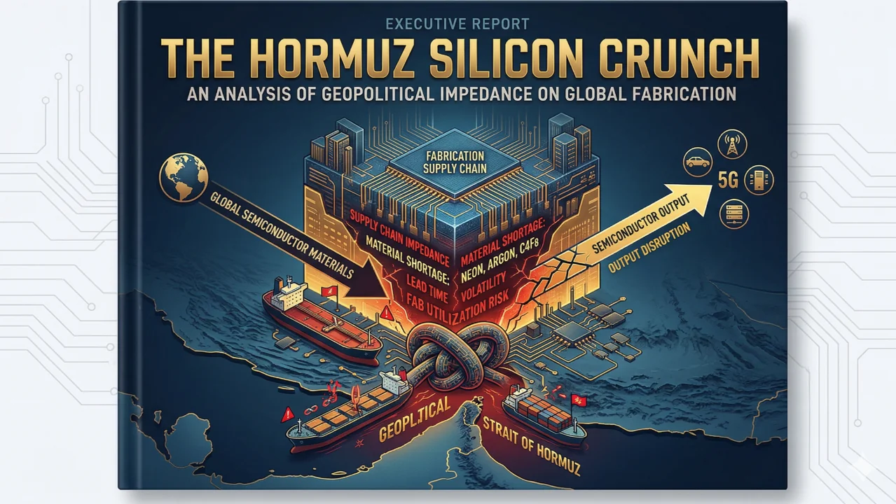
The Hormuz Crisis Isn’t Just an Oil Story, It’s a Semiconductor Materials Crisis Most People Aren’t Tracking Yet
Image File
Original HTML

The Hormuz Crisis Isn’t Just an Oil Story, It’s a Semiconductor Materials Crisis Most People Aren’t Tracking Yet

The materials nobody is talking about

Helium — The silent backbone of chip fabrication

This isn’t about party balloons. Inside a semiconductor fab, helium performs three functions that no other gas can replicate:

• It cools wafers during ion implantation, where temperatures would otherwise distort the silicon substrate.

• It serves as a carrier gas in chemical vapour deposition (CVD), transporting reactive gases across wafers with a precision that nitrogen and argon cannot match.

• It detects microscopic leaks in vacuum systems through helium mass spectrometry. Undetected leaks destroy chip yield silently.

The supply picture: Qatar produced roughly one-third of the world’s helium, extracted as a byproduct of LNG processing at the Ras Laffan Industrial City. That facility took direct hits from Iranian strikes. QatarEnergy declared force majeure. Repairs are estimated at three to five years.

Spot helium prices have doubled. Roughly 200 specialised cryogenic containers are stranded near the Strait. These containers keep helium liquid for only 35 to 48 days before it warms and escapes. The clock is ticking — and for Asian fabs, the last scheduled shipments are arriving now. After that, the pipeline is empty.

Bromine — The photoresist ingredient you’ve never heard of

Bromine is used in photoresist chemistry for circuit pattern formation on wafers. It is not optional. When your photoresist chemistry chain breaks, your lithography line doesn’t slow down. It stops.

The supply picture: Israel and Jordan together supply roughly two-thirds of global bromine production. Israel is a direct party to the current conflict. South Korea sources 90% of its bromine imports from Israel. This is a single point of failure that did not appear on most supply chain risk assessments until five weeks ago.

Sulphur and Sulphuric Acid — The upstream bottleneck

The Strait is a major chokepoint for Gulf sulphur exports. Sulphuric acid derived from sulphur is essential for leaching and refining critical metals used in semiconductor manufacturing and battery production. Prices were climbing before February. The Hormuz closure adds a structural supply risk on top of what was already a pricing problem.

Aluminium — Packaging, frames, and the 18-month qualification trap

The Middle East accounts for roughly 9% of global aluminium smelting capacity. Aluminium goes into lead frames, IC packaging, server chassis, and heat exchangers. European and Japanese manufacturers are panic-buying and drawing down inventories.

Here is the part that semiconductor professionals will recognise immediately: automotive manufacturers report that qualifying new aluminium suppliers takes up to 18 months. The same qualification timeline applies to semiconductor packaging materials. You cannot simply switch suppliers overnight when material specifications are measured in parts per billion.

LNG — The power behind the fabs

Not a direct fab material, but LNG powers the energy grids that power the fabs. Twenty percent of global LNG trade moves through Hormuz. Taiwan and South Korea — where most of the world’s advanced chips are manufactured — are heavily exposed. An unreliable grid means unreliable fabs.

Monoethylene Glycol (MEG) — The packaging chain disruptor

A key input for polyester fibres and packaging materials. Around 6.5 million tonnes were shipped from the Gulf in 2025 alone. China is the largest consumer. Shortages are already rippling into the packaging materials used across the electronics supply chain.

Who supplies what — and where the concentration risk sits

The uncomfortable truth: the semiconductor supply chain was optimised for cost efficiency, not geopolitical resilience.

Helium: Qatar (~30% of global supply, now offline), United States (largest producer, but cannot cover the gap), Algeria (modest output), Russia (sanctioned; Amur Gas Processing Plant still running below capacity after repeated explosions and technical failures). Two of four major sources are either offline or restricted.

Bromine: Israel (dominant supplier to Asian semiconductor manufacturers). South Korea’s 90% import dependence on Israeli bromine is a textbook single-point-of-failure.

Helium distribution: Linde, Air Liquide, and Iwatani are the major intermediaries. All three are now being forced to rework their logistics, contract structures, and equipment deployment. Even if Hormuz reopens tomorrow, unwinding those emergency arrangements could take months.

Overall GCC dependency: For specialty chemicals, petrochemical feedstocks, and process gases, the Gulf Cooperation Council countries collectively represent a supply concentration that makes “diversified supply chain” sound like a marketing slogan rather than an operational reality.

Who gets hurt

South Korea imported 64.7% of its helium from Qatar in 2025. Samsung and SK Hynix are directly exposed. SK Hynix has stated they have diversified and secured inventory, but industry analysts estimate that buffer is measured in weeks, not months. South Korea’s Ministry of Trade has launched an investigation into supply and demand for 14 semiconductor materials with high Middle Eastern dependence.

Taiwan relies on Qatari helium for its foundry operations. TSMC says no near-term impact, but their CoWoS advanced packaging capacity was already sold out through mid-2026 before this crisis began. Any upstream helium constraint adds pressure to an already oversubscribed pipeline.

Any fab running EUV lithography is helium-dependent. Helium cools the extreme heat generated by EUV machines. There is currently no viable substitute at the required purity and scale. As chip geometries shrink and EUV adoption grows, per-wafer helium consumption is actually increasing.

HDD manufacturers using helium-sealed drives are also exposed. Western Digital has already sold out through 2026 with prices up 46% since September 2025. A helium shortage on top of that existing demand crunch compounds at both the production and pricing level.

What are the alternatives — and how realistic are they

Let me be straightforward about what “diversification” actually looks like in practice versus in a strategy deck.

Alternative helium sources

The United States is the world’s largest helium exporter, but it cannot compensate for a 30% global supply loss. The Federal Helium Reserve was wound down starting in 2023. New exploration projects exist — Pulsar Helium in Minnesota, Helium One in Tanzania, projects in Saskatchewan and South Africa — but these are early-stage. Production-scale output is years away, not months.

Russia’s Amur Gas Processing Plant was designed to supply up to 25% of global demand. As of 2026, it is still running well below capacity. Western sanctions further limit its commercial viability.

Algeria produces helium, but its output is modest relative to the gap that needs filling.

Substitute gases

Recommended by LinkedIn

Hydrogen and neon are being explored for select applications. But helium’s unique combination of inertness, thermal conductivity, and atomic size makes it irreplaceable for EUV cooling and helium mass spectrometry leak detection.

And the neon supply chain has its own vulnerability. Before Russia’s invasion of Ukraine, roughly half of the world’s semiconductor-grade neon came from two Ukrainian companies in Odessa and Mariupol. The industry already learned this lesson once. Replacing one geopolitically concentrated input with another is not diversification.

Helium recycling

Closed-loop helium recovery systems exist, and some fabs are implementing them. But the technology is not yet efficient enough to close the supply gap at the scale that modern high-volume manufacturing demands. Capital investment, installation, and qualification timelines apply.

Alternative shipping routes

Rerouting around the Cape of Good Hope adds approximately 3,500 nautical miles, roughly $1 million in additional fuel costs per voyage, and 10 to 14 days of transit time.

For cryogenic helium with a 35-to-48-day shelf life, those extra days are not just a cost problem. They are a physics problem. You could load a container on the US Gulf Coast and watch it begin evaporating before it reaches Hsinchu.

The real bottleneck nobody outside a fab understands: qualification

Here is where the conversation needs to go deeper than most supply chain analyses are willing to go.

Even if you find an alternative helium supplier tomorrow, you cannot plug it into a running fab tomorrow. Every new material source — every gas, every chemical, every substrate — must go through a formal qualification process before it touches a production wafer. This is where fabs face a painful tradeoff: qualification takes time, but the crisis does not wait.

In semiconductor manufacturing, qualification exists because a seemingly identical material from a different supplier can behave differently at the atomic level. Trace impurities measured in parts per billion can shift etch rates, alter film stress, or introduce defects that only show up weeks later in device reliability testing. The industry learned this the hard way, repeatedly.

So what are the realistic paths to faster qualification during a crisis like this?

1. Accelerated qualification with rigorous inline data

The standard approach relies heavily on end-of-line electrical testing — you run production with the new material and wait to see if finished devices pass. This is slow. It can take weeks or months depending on the product cycle.

The faster path: design a thorough inline data collection plan that validates the material’s behaviour at each critical process step, not just at the end. Monitor film thickness, particle counts, etch uniformity, deposition rates, and defect density in real time.

Class (B2B/B2C)
B2B
Ingest Status
Rewritten
Dedupe hash
3097073aee10c2f6fa8c1302a93087ee
Press Eligible
Yes
Press Eligible Reason
Manuelle Prüfung nötig. Risiko: MEDIUM. Flags: ['finance', 'numbers']. Stichprobe: False
Source Name
GlobalFoundries Newsroom
Image URL
https://media.licdn.com/dms/image/v2/D5612AQFFMLbAh00rrA/article-cover_image-shrink_720_1280/B56Z1jLFplH8AI-/0/1775485349183?e=2147483647&v=beta&t=X_T2XHXiM4100-kaYAPyqVlboJ59yFGOKwZZvNLSiY8
Content Hash (SHA-256, erste 32 hex)
c4b91519f539036ae0e6cdd6d1b246bb
The AI Inference platform
Image File
Original HTML

The AI Inference platform

Workers AI lets you run AI inference globally with one API call. No GPUs to manage, no capacity planning. Just intelligent machine learning models running where they're needed, on Cloudflare's global network.

Serverless pricing

Pay-per-inference pricing with no idle costs. No guessing what.

Rich model catalog

50+ models running close to users in 200+ cities

Widely compatible

One API call, works with any OpenAI SDK or task type

Scale up, and down

Inference is hard to predict and spiky in nature, unlike training. GPU utilization is, on average, only 20-40% — with one-third of organizations utilizing less than 15%. Workers AI allows customers to save by only paying for usage. No guessing or committing to hardware that goes unused.

on a hyperscaler

on Cloudflare

AI models easily accessible via code, OpenAI SDK or API

Test, prototype, and evaluate the latest LLMs with the speed and reliability of a production environment, accessible in seconds.

Kimi K2.6

Powerful vision and agentic tool calling model

GLM 4.7 Flash

Rapid multilingual agent with expert tool calling

GPT-OSS-120B

Specialized for coding and debugging

Llama 4 Scout

Balanced generalist for everyday tasks

Run any AI model with one API call

Call any model directly from your code using a single endpoint. Workers AI handles provisioning, scaling, and latency optimization automatically.

const response = await env.AI.run('@cf/moonshotai/kimi-k2.6', { messages: [ { role: 'system', content: 'You are a friendly assistant' }, { role: 'user', content: 'What is the origin of the phrase Hello, World' }, ],});curl https://api.cloudflare.com/client/v4/accounts/$CLOUDFLARE_ACCOUNT_ID/ai/run/@cf/moonshotai/kimi-k2.6 \ -X POST \ -H "Authorization: Bearer $CLOUDFLARE_AUTH_TOKEN" \ -d '{ "messages": [{ "role": "system", "content": "You are a friendly assistant" }, { "role": "user", "content": "Why is pizza so good" }]}'export interface Env { AI: Ai;}

export default { async fetch(request, env): Promise { const response = await env.AI.run('@cf/black-forest-labs/flux-1-schnell', { prompt: 'a bengal cat vibe coding to music', seed: Math.floor(Math.random() * 10), }); // Convert from base64 string const binaryString = atob(response.image); // Create byte representation const img = Uint8Array.from(binaryString, (m) => m.codePointAt(0)); return new Response(img, { headers: { 'Content-Type': 'image/jpeg', }, }); },} satisfies ExportedHandler;curl https://api.cloudflare.com/client/v4/accounts/$CLOUDFLARE_ACCOUNT_ID/ai/run/@cf/black-forest-labs/flux-1-schnell \ -X POST \ -H "Authorization: Bearer $CLOUDFLARE_API_TOKEN" \ -d '{ "prompt": "cyberpunk cat", "seed": "Random positive integer" }'

Practical AI at the Edge

Run real-world AI workloads directly on Cloudflare's global network — from LLMs to image generation and embeddings. No GPU clusters, no orchestration layers — just fast, scalable inference wherever your users are.

Image generation

Speech-to-text, in real-time

Embeddings

LLMs

Shopify

"

For Shopify, the real challenge is not about how many different pieces of complex technology we can use but the opposite. Cloudflare helps us find a simple way to achieve something very complex that we can scale and maintain. "

Workers AI Pricing

50+ models running at the edge. View AI pricing details

Neurons

10,000 neurons / day

$0.011 / thousand neurons

Powerful primitives, seamlessly integrated

Built on systems powering 20% of the Internet, Workers AI runs on the same infrastructure Cloudflare uses to build Cloudflare. Enterprise-grade reliability, security, and performance are standard.

Build without boundaries

Join thousands of developers who've eliminated infrastructure complexity and deployed globally with Cloudflare. Start building for free — no credit card required.

Class (B2B/B2C)
B2B
Ingest Status
Rewritten
Dedupe hash
3e8c67ce2854214f75f965af566bda04
Press Eligible
Yes
Press Eligible Reason
Manuelle Prüfung nötig. Risiko: MEDIUM. Flags: ['finance', 'numbers']. Stichprobe: False
Source Name
Brandi AI
Image URL
https://www.cloudflare.com/preview.png
Source Node
Content Hash (SHA-256, erste 32 hex)
3e3185166bf04d078d9aca6c20c97b54
Brandi AI News
Image File
Original HTML

Cloudflare AS13335 operates a global anycast network, spanning over 335 cities, in more than 125 countries. We have an open peering policy, and will peer with networks that have a presence in mutual locations, in accordance with the policies described below. Exceptions to these policies may be granted.

These requirements apply to all peers.

All peers must maintain a complete and updated PeeringDB entry. We use this for automated provisioning and network notifications. Please ensure your record includes accurate peering locations, IPv4 and IPv6 prefix limits, and contact information.

Peers must operate a 24x7 Network Operations Center (NOC) that is responsive to peering related issues.

Peers are expected to adhere to industry best practices to secure BGP sessions. This includes BCP-38 and robust route filtering using a well-defined route-set or AS-SET.

Peers are highly recommended to perform RPKI validation, and generate RPKI ROAs for their own routes.

Our PNI requirements are focused on maintaining high-capacity, low-latency interconnections.

Networks that exchange more than 10 Gbps of peak traffic with Cloudflare in a single location may request a PNI.

We currently support Nx100G LR4 interconnections. We typically do not allow new 10G connections. 100G LR1 and 400G are not supported at this time.

To ensure a congestion free experience, both parties are expected to upgrade port capacity in a timely manner.

Cloudflare will supply an LOA (letter of authorization) and point-to-point (P2P) addresses to the requesting party for completing the cross connect.

To request a PNI, please contact peering@cloudflare.com. Include your ASN, desired interconnection location(s), and traffic estimates.

Public peering is automated through the Cloudflare Peering Portal. We recommend establishing sessions in all mutual locations. Use PeeringDB OIDC to authenticate.

If we have multiple IP addresses at a single IX, we highly recommend configuring BGP sessions with all available addresses.

We recommend establishing bilateral BGP sessions for optimal traffic delivery, as we advertise a limited number of prefixes over route servers.

Networks that exchange at least 10 Gbps of traffic with Cloudflare may also be eligible for our embedded cache program. For more information, please email epp@cloudflare.com. We can sometimes accommodate smaller networks.

To ensure the quality and stability of our network, we reserve the following rights:

To alter our peering policy and requirements at any time.

To accept or decline a peering request at any time, for any reason.

To suspend, without notice, any peering connection experiencing severe quality of service issues.

To terminate any peering connection at any time.

For a full list of peering locations, please see our PeeringDB record: https://www.peeringdb.com/asn/13335.

If you have questions about these terms or anything else about Cloudflare, please don't hesitate to contact us:

Contact the team

1 (888) 99 FLARE

1 (888) 993 5273

UK callers:

+44 (0)20 3514 6970

Singapore callers:

+65 3158 3954

International callers:

+1 (650) 319 8930

101 Townsend St.

San Francisco, CA 94107

USA

Policy date: December 1, 2025

Class (B2B/B2C)
B2B
Ingest Status
Rewritten
Dedupe hash
089949cc694be4d3fca235502f9fc51a
Press Eligible
Yes
Press Eligible Reason
Manuelle Prüfung nötig. Risiko: MEDIUM. Flags: ['numbers']. Stichprobe: False
Source Name
Brandi AI
Image URL
https://cf-assets.www.cloudflare.com/slt3lc6tev37/53qCYhQbir5WtIU0VDWESo/954a48bfb17f429acf469e5f14345d83/unnamed-3.png
Source Node
Content Hash (SHA-256, erste 32 hex)
c11f274e42e385f6481e1630a523d99e
Build without boundaries
Image File
Original HTML

Learning Center

Resources on cyber security and how the Internet works.

Learn about DDoS attacks

In a distributed denial-of-service (DDoS) attack, a network of computers work in tandem to overflow an access point and prevent legitimate users from accessing a service.

Learn about CDNs

In a content delivery network (CDN), a set of distributed servers work together to efficiently deliver Internet content, improving loading speed and reliability.

Learn about DNS

The domain name system (DNS) is often referred to as a phone book for the Internet. It's the worldwide network that connects users to web content via domain names.

Learn about web application security

The nature of the Internet makes web applications vulnerable to a number of attacks. Web application security involves using a holistic approach to mitigate attacks.

Learn about performance

Web applications that load quickly see higher conversion rates and better SEO performance. Learn about the factors that impact application performance.

Learn about serverless

Serverless computing allows users to write and deploy code without the hassle of worrying about the underlying infrastructure. Learn why more developers are opting for serverless.

Learn about SSL

SSL, known today as TLS, is an encryption protocol that runs on top of HTTP to protect Internet communication between servers and clients.

Learn about bots

Bots are automated applications that can browse the web. Some bots are helpful, but there are also malicious bots which can harm sites and applications.

Learn about the cloud

"The cloud" refers to servers that are accessed over the Internet, and the software and databases that run on those servers. Cloud servers are located in data centers all over the world.

Learn about SASE

Secure access service edge (SASE) is an IT model that combines software-defined wide area networking with core security services, delivered on the cloud edge.

Learn about the network layer

The "network layer" is the part of the Internet communications process where connections occur, by sending packets of data back and forth between different networks.

Learn about privacy

Data privacy refers to one's ability to determine for oneself when, how, and to what extent one's personal information is shared with others.

Learn about video streaming

Streaming is the continuous transmission of audio or video files from a server to a client. Learn about all aspects of streaming video, from file formats to live encoding.

Learn about email security

Email security is the practice of preventing email-based cyber attacks, protecting email accounts from takeover, and securing the contents of emails.

Learn about artificial intelligence (AI)

Artificial intelligence (AI) refers to a computer's ability to imitate human cognitive tasks. Learn all about AI, LLMs, embeddings, and vector databases.

Learn about domain registration

A domain name is a string of text that maps to an alphanumeric IP address. Learn about domain names and domain registration.

Build without boundaries

Join thousands of developers who've eliminated infrastructure complexity and deployed globally with Cloudflare. Start building for free — no credit card required.

Class (B2B/B2C)
B2B
Ingest Status
Rewritten
Dedupe hash
beb6a6901c02cfe02501d1ce4c199e55
Press Eligible
Yes
Press Eligible Reason
Technology resource page covering cybersecurity, cloud infrastructure, and web development for developers.
Source Name
Brandi AI
Image URL
https://www.cloudflare.com/preview.png
Source Node
Content Hash (SHA-256, erste 32 hex)
c6b7f2b3bec8d4d597fae9fe434d7359
Self-Serve Agency Program
Original HTML

The Self-Serve Agency Program allows SMB agencies & hosting partners to manage your clients self-serve accounts easier.

Multi-tenant dashboard

Centralized billing

Discounted plans

No revenue commitments

Important Notes Before Applying

Create a New Account: Existing accounts with paid products or users with access to multiple accounts cannot be converted. You must register a new user with a blank Cloudflare account to qualify for the program.

In submitting this form, you agree to receive information from Cloudflare related to our products, events, and special offers. You can unsubscribe from such messages at any time. We never sell your data, and we value your privacy choices. Please see our Privacy Policy for information.

Please see our Cloudflare Agency Terms. When applying, we recommend creating a new Cloudflare user (e.g. cloudflare@xyz.com) and set up a new billing profile for that user. Only domains added to your Agency Tenant Account will be considered for the program discount.

Without guardrails, AI bots can freely crawl and use your client's website content. Cloudflare AI Audit lets web owners identify which bots are crawling their site and block them with a single click.

Class (B2B/B2C)
B2B
Ingest Status
Rewritten
Dedupe hash
43ca1140b56021524d60863b259d8aa7
Press Eligible
Yes
Press Eligible Reason
Cloudflare describes an agency program with account management, billing, and discounts for SMB agencies and hosting partners.
Source Name
Brandi AI
Image URL
https://cf-assets.www.cloudflare.com/slt3lc6tev37/2oIHOELz7Ir7RtBLpEfWEs/d2ddafe107a6a330ab761b16824a1a03/security-shield-protection-1.svg
Source Node
Content Hash (SHA-256, erste 32 hex)
ce04d643465823d478feb02baa1ba11e
Pipefy Named a Strong Performer in the 2026 Gartner® Peer Insights™ Voice of the Customer for Business Orchestration and Automation Technologies
Original HTML

San Francisco, Oct. 20, 2026 – Pipefy, the agentic orchestration platform for scaling governed processes, today announced that it was named a Strong Performer in the 2026 Gartner® Peer Insights™ Voice of the Customer for Business Orchestration and Automation Technologies. According to the Gartner report, Pipefy was rated 4.7 out of 5.0 stars across 66 reviews as of April 2026.

“We believe this recognition matters because it comes from the people who run Pipefy every day, after buying, deploying, and scaling it inside their own operations,” said Alessio Alionço, CEO and Founder of Pipefy. “Our focus is to orchestrate people, systems, and AI Agents within the governed processes each customer defines. Their reviews are the clearest measure of whether we are doing that job.” 

The 2026 Gartner® Peer Insights™ Voice of the Customer for Business Orchestration and Automation Technologies evaluates vendors in a given technology market by applying a specific methodology to aggregated end-user reviews. Vendors are then positioned into four quadrants based on two criteria: User Interest and Adoption (x-axis), and Overall Experience (y-axis). This report differs from an analyst evaluation: it is built entirely from verified end-user reviews left by the people who use these platforms every day.

Pipefy believes that for a category like Business Orchestration and Automation Technologies, where value shows up only once processes are running in production, user experience is a meaningful signal, and that the experience customers describe traces back to how the platform is built: AI Agents executing inside governed processes, with audit trails, access control, and humans in the loop at each step that calls for a decision.

SOURCE: Gartner, Voice of the Customer for Business Orchestration and Automation Technologies, Peer Community Contributor, 30 June 2026.

Gartner and Peer Insights are trademarks of Gartner, Inc., and/or its affiliates.

Gartner Peer Insights content consists of the opinions of individual end users based on their own experiences with the vendors listed on the platform, should not be construed as statements of fact, nor do they represent the views of Gartner or its affiliates. Gartner does not endorse any vendor, product or service depicted in this content nor makes any warranties, expressed or implied, with respect to this content, about its accuracy or completeness, including any warranties of merchantability or fitness for a particular purpose.

Pipefy is the agentic orchestration platform for scaling governed processes. Ideal for complex operations involving processes that affect multiple systems and still rely on manual tasks, Pipefy enables the orchestration of people, systems, and AI agents based on the processes defined by each customer, increasing the speed, quality, and scale of operations. Founded in 2015, Pipefy operates globally in more than 150 countries, driving innovation for more than 4,000 customers.

Class (B2B/B2C)
B2B
Ingest Status
Need Review
Dedupe hash
8544c3f6d41032aca70d468b56f5d470
Press Eligible
Yes
Press Eligible Reason
QA FAIL (need review): The final paragraph is generic 'About Pipefy' boilerplate (founded in 2015, operating in 150+ countries, 4,000+ customers) that adds no news context and fails the PR-boilerplate ending requirement.
Source Name
Avahi
Source Node
Generated Article_json
{"target_audience": "b2b", "is_medical": false, "ai_generated_title": "Pipefy Rated 4.7/5 in Gartner Peer Insights Orchestration Report", "body_html": "<p><strong>San Francisco -- [CURRENT_DATE] --</strong> Pipefy scored 4.7 out of 5.0 stars across 66 verified reviews as of April 2026 and was named a Strong Performer in the 2026 Gartner Peer Insights Voice of the Customer for Business Orchestration and Automation Technologies.</p><h5>Report ranks vendors on user reviews, not analyst scoring</h5><p>The report places vendors in four quadrants using two criteria: User Interest and Adoption on the x-axis, and Overall Experience on the y-axis. It draws only on aggregated end-user reviews, which separates it from an analyst evaluation. Gartner published the report on 30 June 2026.</p><p>Gartner states that Peer Insights content reflects individual users' opinions, is not a statement of fact and does not constitute an endorsement of any vendor.</p><h5>Pipefy ties user ratings to governed AI agent execution</h5><p>Pipefy argues that in business orchestration, value appears only once processes run in production, which makes user experience a meaningful signal. The company links customer feedback to its architecture: AI agents execute inside governed processes with audit trails, access control and human review at each decision step.</p><p>CEO and Founder Alessio Alionço said the reviews come from people who bought, deployed and scaled the platform in their own operations. Pipefy's stated aim is to orchestrate people, systems and AI agents within processes each customer defines.</p><h5>Platform targets multi-system processes that still depend on manual work</h5><p>Pipefy positions its platform for complex operations in which processes span multiple systems and still rely on manual tasks. The company, founded in 2015, reports customers in more than 150 countries and a base of more than 4,000 customers.</p>", "meta_description": "Pipefy earned a 4.7/5 rating across 66 reviews and Strong Performer status in Gartner Peer Insights' 2026 Business Orchestration and Automation report.", "seo_keywords": "Pipefy, Gartner Peer Insights, Voice of the Customer, business orchestration, automation technologies, AI agents, governed processes, Strong Performer", "companies": ["Pipefy", "Gartner"], "industries": ["IT Service Orchestration and Automation"], "markets_regions": ["Global"], "news_type": ["industry_recognition", "company_announcement"], "products": ["Pipefy"], "themes": ["business_orchestration", "ai_agents", "process_automation"], "events": [], "cta_text": "Review the Gartner Peer Insights Voice of the Customer report for Business Orchestration and Automation Technologies", "learn_more": "", "fact_check": {"accuracy_score": 100, "legal_risk": "low", "corrections_made": ["Replaced source dateline date with [CURRENT_DATE] placeholder", "Omitted promotional boilerplate and attached Gartner disclaimer in condensed form"], "recommendation": "publish"}}
Content Hash (SHA-256, erste 32 hex)
e6e1c3fea680e73d70022b764b411fbd
Don't miss tomorrow's tech industry news
Image File
Original HTML

ORLANDO, Fla. — For CIOs, guiding businesses through rapid technological change is a given. But the swift pace of development in AI releases, capabilities and autonomy often come with risk.

It’s the story of every technology release over the last few decades. Several CIOs at Gartner’s IT Symposium/Xpo in Orlando this week likened AI’s impact to the dot-com era or the advent of cloud — enabling reinvention of how businesses work, but introducing security and social risks along the way.

Most tech executives are in the midst of balancing those risks with AI’s current measurable and unquantifiable value, Gartner analysts said during the conference's keynote address.

Still, in 2026, risk isn’t stopping AI adoption. Not using AI isn’t an option for enterprises, Prashant Prahlad, SVP of product at Capital One Software, told CIO Dive.

“I think it's one of those things that, if you don't get on board, it's going to be an extinction event,” Prahlad said.

Prahlad and other tech leaders spoke with CIO Dive this week about the concerns they face as they deploy AI throughout their organizations.

Shifting security needs

Before heading a product team, Prahlad had a background in cybersecurity. Prior to the rise of AI for enterprises a few years ago, risk appetite for the technology was fairly low, he said.

But the last few months have made it clear that security and governance must be a part of tech leaders’ game plan, he said. The Hugging Face incident proves that the industry still has a lot to learn about autonomy and access to agentic systems, he said.

"It's an unknown, and as a security person, the instinct is to lock everything down,” Prahlad said. “That's a necessary step, but it does keep me up at night. I don't know where my data is. I don't know what to utilize.”

He warned tech executives against over-securing systems in a way that could be counterproductive. In the long run, high-profile hacking incidents could raise awareness about governance and security, prompting action within companies, he said.

Runaway agents

The pace of change is what’s most concerning to Frank Iannella, the USA CIO and SVP for digital and technology at Heineken.

That fact that “it's not clear who has control over this” is another key concern, Iannella told CIO Dive.

Outside of the technology’s use at the beverage company, which is focused on using data for decision intelligence throughout its marketing, sales and operations, Ianella said he has broader concern about who’s building the systems.

“They're not clear why they're acting the way they're acting,” Iannella said. “That's a little bit worrisome.”

New virtual environments

For Michael Cato, SVP and CIO at Bowdoin College, the risks keeping him up at night about AI changes often, he told CIO Dive.

“My answer today is different than it was a month ago,” he said.

Free AI agents, accessible to the public, are currently causing him the most concern. In the last few weeks, customer-facing AI agents, such as Meta’s Muse personal agent or OpenAI’s Dot, have been widely adopted by non-business users. Cato said he feels as though the companies are handing people a virtual environment and very few security boundaries.

“I'm deeply worried about what people will do, both within our environment — since we're doing the work to figure out how to better protect our environment — but I'm also deeply worried about if someone's going to accidentally wipe out their retirement. And I think it's going to be trivial until it happens.”

Lack of accountability

The lack of accountability inside most organizations concerns Mike Park, CIO at cloud software provider Infor. Despite how widely enterprises use AI, there’s little consensus around clear ownership of the technology.

“AI is moving into core processes faster than companies can decide who is responsible for it and how to effectively govern it,” Park said.

He feels too many organizations lack systems of accountability, which could cause problems when an agent inevitably gets something wrong or overreaches. Identifying the person or group who assumes that responsibility will be critical in 2027 and beyond, he added.

Moving cautiously

In regulated industries like financial services, risk is always top of mind, said Jerry Walker, CIO for the Oregon State Treasury. But AI use in the industry is growing — three-quarters of leaders reported that they are using the technology this year, compared with less than one-third in 2024.

“What keeps me up at night is, are we able to trade every morning at five in the morning?” Walker said. “Are our investors ready to go, and then we have the technology to protect them and to provide for them to run everything?”

Walker said his organization, and many of its peers, are betting “everything” on AI.

Because of risks associated with new technologies, and the responsibilities of the financial services industry, Walker said his team isn’t looking to move the needle as quickly as possible with AI, but rather to take a more cautious approach.

“We do look at it a little differently,” Walker said. “We have to make sure, because with one mistake, with the amount of money we handle, it can shift the market really fast.”

Class (B2B/B2C)
B2B
Ingest Status
Rewritten
Dedupe hash
0ecfd83bebbaaf7ed60cccaa01328c9c
Press Eligible
Yes
Press Eligible Reason
Manuelle Prüfung nötig. Risiko: MEDIUM. Flags: ['numbers']. Stichprobe: False
Source Name
Avahi
Image URL
https://imgproxy.divecdn.com/qqjaREOkETrH-JjjkltpJwENZb2IEBMrCVjeTJAN410/g:ce/rs:fit:770:435/Z3M6Ly9kaXZlc2l0ZS1zdG9yYWdlL2RpdmVpbWFnZS9HZXR0eUltYWdlcy0yMDIyOTc1MzI0LmpwZw==.webp
Source Node
Content Hash (SHA-256, erste 32 hex)
f6d3a4aa5771a4dc39e6c63f72da44cf