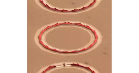
PISCATAWAY – November 02, 2026 -- Researchers report that the optical structure beneath a 10 nm gold film changes how laser-induced dewetting unfolds, offering a new lever for controlling nanostructure formation in metallic thin films, according to a study in IEEE Journal of Selected Topics in Quantum Electronics.
Two of four substrates produced previously unreported dewetting features
The team fabricated four samples with identical chemical compositions but different optical structures, varying the thickness of the underlying silica and gold layers. Two samples showed the expected solid-state dewetting behavior. The other two exhibited broad nano- and micron-scale particle size distributions and complex spatial patterns not reported before.
Simulations rule out local electric field variations as the cause
Finite-element simulations excluded local electric field variations as the explanation. The authors conclude that nonlocal optical effects act alongside thermal, capillary, and fluid dynamic effects. The nonlocal environments are created with optically engineered nanophotonic materials such as optical cavities.
Size and distribution control remains a bottleneck in laser patterning
Laser-induced dewetting offers greater precision, speed, and flexibility than thermal dewetting and is a promising route for patterning metallic thin films. In plasmonic color laser printing and substrate-engraved metasurfaces, controlling the size and distribution of the resulting nanostructures remains a major challenge. In low-emissivity window coatings and nanoscale plasmonic devices, dewetting is undesirable because it shortens coating lifetime and degrades device performance.
Corresponding author Mikhail A. Noginov said engineering the underlying optical cavity adds "more flexibility in controlling dewetting dynamics" and can help reduce dewetting where laser-induced damage is undesirable.
The study went online on Feb. 23, 2026, and appeared on May 1, 2026, in Volume 32, Issue 3 of the journal.